
There is a dashcam on the market that requires an external adapter for testing. During power-on testing, it was found that the radiation exceeded the limit at specific frequencies: 84 MHz, 144 MHz, and 168 MHz. The analysis of the radiation source revealed the following details:

Upon investigation, the dashcam only has one PCB, and on the board, there’s a 12 MHz crystal oscillator. Interestingly, the frequencies at which radiation exceeded the limit were multiples of 12 MHz. Further analysis of the machine’s potential EMI radiation sources—specifically the screen and camera—revealed that the LCD-CLK is 33 MHz and the camera MCLK is 24 MHz.
Using the process of elimination, it was discovered that even with the camera removed, the excessive radiation points still existed. However, when the 12 MHz crystal was shielded, the radiation levels dropped. This led to the conclusion that the 144 MHz excessive radiation was linked to the crystal. The PCB layout looked like this:
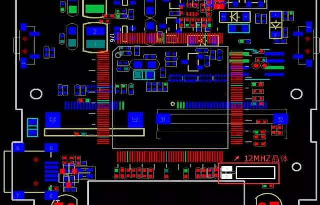
Upon reviewing the PCB layout, it was found that the 12 MHz crystal oscillator was placed directly at the edge of the PCB. When the product was placed in the test environment for radiation emission, the high-speed components of the device and the reference ground in the lab created capacitive coupling, resulting in parasitic capacitance. This led to common-mode radiation. The greater the parasitic capacitance, the stronger the common-mode radiation. Essentially, the parasitic capacitance arises from the electric field distribution between the crystal and the reference ground. When the voltage between the two remains constant, the more the electric field is distributed between them, the stronger the field and parasitic capacitance. The electric field distribution of the crystal placed at the PCB edge compared to the center of the PCB is as follows:
When the crystal oscillator is positioned in the center of the PCB or away from the edge, the PCB’s ground plane helps contain most of the electric field between the crystal and the ground, minimizing the electric field distribution to the reference ground. As a result, radiation emissions are significantly reduced.
Based on this analysis, the crystal oscillator was moved inward, keeping it at least 1 cm away from the PCB edge. Copper was added to the PCB layer within 1 cm of the crystal, and this copper was connected to the PCB ground plane through vias. The test results after the modification showed a significant improvement in the radiation emissions, as shown in the frequency spectrum graph below:

If, for design reasons, the crystal oscillator must be placed at the edge of the PCB, it’s recommended to place an additional working ground line along the edge of the PCB traces and increase the number of vias to connect this working ground line to the ground plane.
Note: This article aims to provide industry insights into crystal oscillators. We apologize for any similarities with other content.